

India-Singapore Comprehensive Strategic Partnership:
Focus on Semiconductors
Amitendu Palit, Mriganika Singh Tanwar
12 September 2024Summary
Cooperation in semiconductors is prominent in India and Singapore’s decision to elevate their ties to a comprehensive strategic partnership. The engagement connects to India’s efforts to become a global semiconductor hub and make regional semiconductor supply chains more resilient.
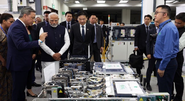
India’s Prime Minister Narendra Modi visited Singapore on 4 and 5 September 2024. This was his first visit to Singapore after being returned to office for a third term in June 2024 and his fifth visit overall.
The visit witnessed the elevation of India-Singapore bilateral ties to a comprehensive strategic partnership. With bilateral ties heading for their 60th anniversary in 2025, the elevation underscores the intent of both countries to cooperate extensively on subjects of mutual strategic interest. Four memorandums of understanding (MoUs) were signed during the visit – on semiconductors, digital technologies, healthcare and skill development. Among these, semiconductor is an area where India is keen to work closely with Singapore in realising its ambition of becoming a global semiconductor manufacturing hub.
The India Perspective
India’s current industrial policy highly emphasises the growth of indigenous semiconductor capacities. Semiconductor or chip-making capacities hold the key to strategic comparative advantages of countries in a world where chips are vital for almost all civilian, economic and military purposes. India, till now, has not been a significant player in the global semiconductor industry landscape which is predominantly influenced by the United States (US), Japan, Taiwan, South Korea and China. New Delhi realises the immense strategic importance of ‘catching up’ with these countries through closer partnerships, including with Singapore, to attain its goal.
The India Semiconductor Mission, announced in 2021, outlines India’s efforts to become a global semiconductor manufacturing hub. The ambition received a boost from several mega-projects to create local chip-making capacities. These include the US$11 billion (S$15.07 billion) joint venture between Tata Electronics and Powerchip Semiconductor (PSMC) of Taiwan to produce a variety of nano-chips in Dholera in Gujarat, an advanced packaging facility of US$3.25 billion (S$4.45 billion) to be built by the Tata Electronics in Jagiroad in Assam and US semiconductor giant Micron Technology’s US$2.75 billion (S$3.77 billion) assembly and testing facility in Sanand in Gujarat.
Supply Chain and Value Addition
A semiconductor supply chain begins with the designing of chips and then to their manufacturing through wafer fabrication, followed by their packaging and testing, and finally assembling them in devices and gadgets. The initial or upstream activities in the chain, such as design and fabrication, are the relatively greater value additive segments in the chain. Among these, designing chips is considerably a research and development (R&D)-intensive function, whereas wafer fabrication, as well as packaging and testing, are more labour-intensive, particularly the latter.
Most semiconductor investments in India are currently concentrating on assembling and packaging, with the notable exception of a few, such as the Tata-PSMC facility in Dholera, which specialises in fabrication. These investments are consequential as India must produce downstream facilities to make chips locally to meet high domestic demand. However, the goal of becoming a semiconductor manufacturing hub and securing a global strategic advantage in the process will require India to attract more investments in R&D-intensive design and fabrication. India has the competencies in design and can exploit the same through effective collaboration with Singapore.
Singapore’s Strategic Importance
Singapore accounts for around 11 per cent of the global market for semiconductors and has several fabrication plants, including large global wafer foundries (for example, Taiwan Semiconductor Manufacturing Company, GlobalFoundries and the United Microelectronic Corporation). Singapore and Malaysia are the only two countries from Southeast Asia that have foundries producing wafers to make chips. Singapore also has several firms producing semiconductor materials and equipment underpinning its success in creating a robust semiconductor ecosystem.
Singapore’s strengths make it a natural partner for India, which is looking for global investments in various segments of the semiconductor supply chain, and also in establishing a capable network of vendors and suppliers to seamlessly support design and fabrication. India is interested in reproducing Singapore’s success in creating a strong semiconductor supplier network comprising local clusters for design, raw materials, components and machinery.
Looking Ahead
The MoU on the India-Singapore Semiconductor Ecosystem Partnership between India’s Ministry of Electronics and Information Technology and Singapore’s Ministry of Trade and Industry establishes a framework for bilateral strategic cooperation. The framework can leverage Singapore’s semiconductor ecosystem to support the growth of identical capacities in India. Both countries have also decided to catalyse private sector partnerships in semiconductor manufacturing through business-to-business engagements. The announced emphasis on policy exchanges in the semiconductor ecosystem, dialogue mechanisms and workforce skill development are all mutually synergistic.
The India-Singapore cooperation in semiconductors will enhance the resilience of regional semiconductor supply chains. It is an important step in India’s efforts to engage with regional partners to enhance collective economic security in strategic and critical industries.
. . . . .
Dr Amitendu Palit is a Senior Research Fellow and Research Lead (Trade and Economics) at the Institute of South Asian Studies (ISAS), an autonomous research institute at the National University of Singapore (NUS). He can be contacted at isasap@nus.edu.sg. Ms Mriganika Singh Tanwar is a Research Analyst at the same institute. She can be contacted at m.tanwar@nus.edu.sg. The authors bear full responsibility for the facts cited and opinions expressed in this paper.
Pic Credit: Twitter
-
 More From :
-
 Tags :
-
 Download PDF